logo
Startseite ProdukteRf-PWB-Brett

2-layer PCB on RF-10 Substrate 20mil Immersion Silver Finish

Bescheinigung
CHINA Bicheng Electronics Technology Co., Ltd zertifizierungen
Kunden-Berichte
Kevin, Empfing und prüfte die Bretter - Dank sehr viel. Diese sind, genau perfekt, was wir benötigten. rgds Reiche

—— Rich Rickett

Ruth, Ich erhielt das PWB heute, und sie sind gerade perfekt. Bleiben Sie bitte eine wenig Geduld, mein folgender Auftrag kommt bald. Mit freundlichen Grüßen von Hamburg Olaf

—— Olaf Kühnhold

Hallo Natalie. Es war, ich befestigt einige Bilder als Ihre Referenz perfekt. Und ich schicke Ihnen folgende 2 Projekte, um zu planen. Dank viel wieder

—— Sebastian Toplisek

Kevin, Dank, wurden sie tadellos gemacht und funktionieren gut. Wie, sind hier die Verbindungen für mein spätestes Projekt, unter Verwendung des PCBs versprochen, das Sie für mich herstellten: Viele Grüße, Daniel

—— Daniel Ford

Ich bin online Chat Jetzt

2-layer PCB on RF-10 Substrate 20mil Immersion Silver Finish

2-layer PCB on RF-10 Substrate 20mil Immersion Silver Finish

Großes Bild :  2-layer PCB on RF-10 Substrate 20mil Immersion Silver Finish

Produktdetails:
Herkunftsort: CHINA
Markenname: Bicheng
Zertifizierung: UL, ISO9001, IATF16949
Modellnummer: BIC-052.V1.0
Zahlung und Versand AGB:
Min Bestellmenge: 1pcs
Preis: USD9.99-99.99
Verpackung Informationen: Vakuumbeutel+Kartons
Lieferzeit: 8-9 Arbeitstage
Zahlungsbedingungen: T/t
Versorgungsmaterial-Fähigkeit: 5000 Prozent pro Monat

2-layer PCB on RF-10 Substrate 20mil Immersion Silver Finish

Beschreibung
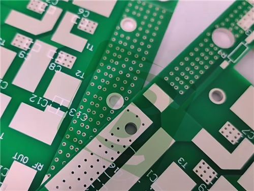
Grundmaterial: Kupferkaschiertes RF-10-Laminat Schichtzahl: 2-layer
Dicke der Leiterplatte: 0,6 mm PCB -Größe: 130 mm × 60 mm (± 0,15 mm)
Kupfergewicht: 1oz (1,4 mil) auf den Außenschichten Oberflächenbeschaffung: Eintauchen Silber
Hervorheben:

2-layer RF PCB board

,

RF-10 substrate PCB

,

20mil immersion silver PCB

2-layer PCB on RF-10 Substrate 20mil Immersion Silver Finish

This 2-layer high-performance PCB is engineered for RF (Radio Frequency) applications, utilizing the advanced properties of RF-10 copper clad laminates to achieve exceptional electrical, thermal, and mechanical performance.


1. PCB Specifications

Parameter Specification
Base Material RF-10 copper clad laminate (ceramic-filled PTFE with woven fiberglass reinforcement)
Layer Count 2 layers (top and bottom copper layers)
Board Dimensions 130mm × 60mm per unit, tolerance ±0.15mm
Trace & Space Specifications Minimum trace width 5 mils, minimum trace spacing 7 mils
Hole Requirements Minimum hole size 0.3mm; no blind vias
Finished Board Thickness 0.6mm
Copper Weight 1oz (1.4 mils or 35μm) for top and bottom layers
Via Plating 20μm thick plating on vias
Surface Finish Immersion silver
Silkscreen & Solder Mask - Top Layer White silkscreen + Green solder mask
Silkscreen & Solder Mask - Bottom Layer No silkscreen or solder mask
Quality Assurance 100% electrical testing prior to shipment


2. PCB Stack-up

Layer Thickness Function
Top Copper Layer (Copper_layer_1) 35μm (1oz) Primary layer for signal traces and component pads
RF-10 Core 20 mils (0.508mm) Dielectric substrate enabling RF capabilities
Bottom Copper Layer (Copper_layer_2) 35μm (1oz) Supports ground planes or additional signal paths


3. Quality Standards

Artwork Format: Gerber RS-274-X, the industry-standard format for PCB manufacturing, ensuring compatibility with most design software and fabrication processes


Quality Certification: Complies with IPC-Class-2 standards, meeting rigorous requirements for performance, reliability, and consistency in commercial and industrial applications


Global Availability: Available for customers worldwide, regardless of country or region, ensuring seamless access to our products


2-layer PCB on RF-10 Substrate 20mil Immersion Silver Finish 0


4. RF-10 Material: Key Features & Advantages

The PCB’s performance is rooted in the superior properties of RF-10 copper clad laminates, a composite of ceramic-filled PTFE and woven fiberglass. Below is a detailed overview of its features and benefits:


4.1 Critical Material Features

RF-10 is optimized for RF applications, with specifications that ensure consistent performance at high frequencies:


-Dielectric Constant (DK): 10.2 ± 0.3 at 10GHz (tight tolerance for predictable signal behavior)


-Dissipation Factor: 0.0025 at 10GHz (ultra-low signal loss, critical for high-frequency RF systems)


-Thermal Conductivity: 0.85 W/mk (unclad) (efficient heat dissipation to prevent component overheating)


-Coefficient of Thermal Expansion (CTE): x = 16 ppm/°C, y = 20 ppm/°C, z = 25 ppm/°C (low expansion to maintain structural integrity under temperature fluctuations)


-Moisture Absorption: 0.08% (minimal water uptake, preventing performance degradation in humid environments)


-Flammability Rating: V-0 (self-extinguishing, meeting safety standards for electronics)


4.2 Core Benefits of RF-10

These features translate to tangible advantages for both design engineers and end-users:


-Size Reduction for RF Circuits: High DK (10.2) allows for smaller circuit footprints, ideal for compact devices like GPS antennas or satellite components


-Exceptional Dimensional Stability: Woven fiberglass reinforcement and low CTE prevent warping or shifting, ensuring alignment with other components


-Tight DK Tolerance: ±0.3 variation ensures consistent signal propagation across the PCB, reducing design iterations


-Enhanced Thermal Management: High thermal conductivity protects sensitive RF components from overheating, extending lifespan


-Strong Copper Adhesion: Bonds well to smooth low-profile copper, minimizing delamination risks and ensuring long-term reliability


-Low Multi-Axis Expansion: x, y, and z CTE values reduce stress on solder joints and components during temperature cycles


-Cost-Effective Performance: Balances high-end RF capabilities with industry-acceptable delivery times and pricing, offering an excellent price/performance ratio


5.Applications

- Microstrip Patch Antennas

- GPS Antennas

- Passive Components (filters, couplers, power dividers)

- Aircraft Collision Avoidance Systems

- Satellite components


In summary, the 2-layer RF-10 PCB combines precise manufacturing, high-quality materials, and industry-compliant design to deliver a reliable, high-performance solution for critical RF applications. Its balance of size, performance, and cost makes it a versatile choice for engineers seeking to optimize their RF systems.


2-layer PCB on RF-10 Substrate 20mil Immersion Silver Finish 1

Kontaktdaten
Bicheng Electronics Technology Co., Ltd

Ansprechpartner: Ms. Ivy Deng

Telefon: 86-755-27374946

Faxen: 86-755-27374848

Senden Sie Ihre Anfrage direkt an uns (0 / 3000)